EVGA Z170 Classified Sub-Zero Overclocking Review
EVGA Z170 Classified
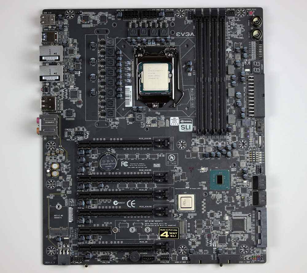
Today we will take a look at the EVGA Z170 Classified motherboard and see just how it does when put under extreme overclocking conditions. Unlike Classified boards of the past, this one is definitely not geared toward the mass population of extreme overclockers who are going to put it under liquid nitrogen. The boards BIOS is very simple in voltage and memory options but as we will see it actually is able to perform very well. This is definitely proven from the fact that EVGA’s own in-house overclocker K|ngp|n uses the board as a platform for constantly setting new world records in the cat and mouse game of competitive benchmarking.
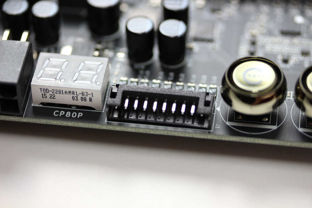
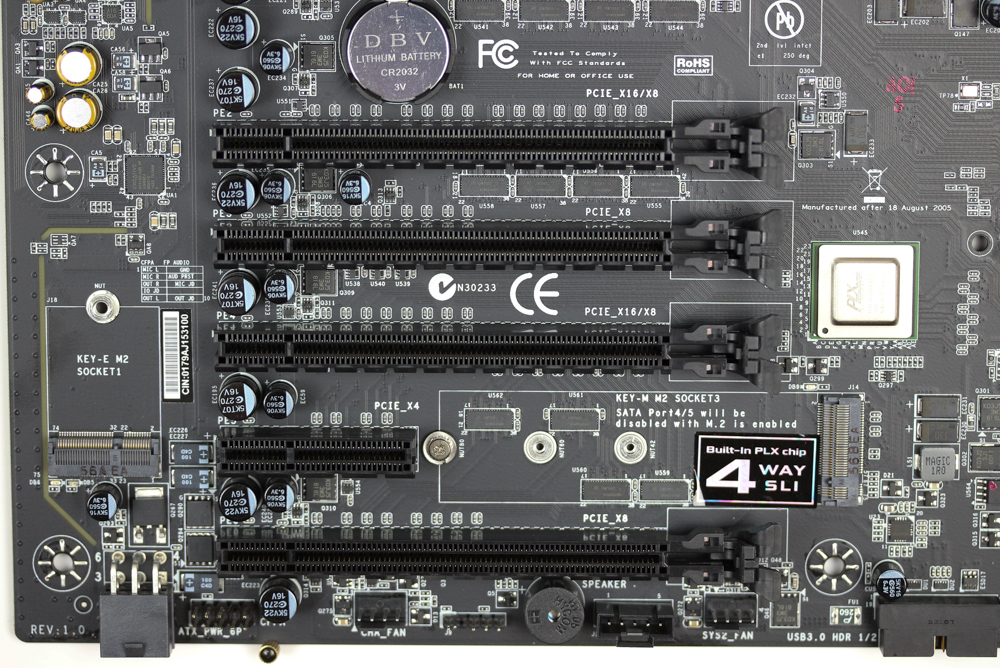
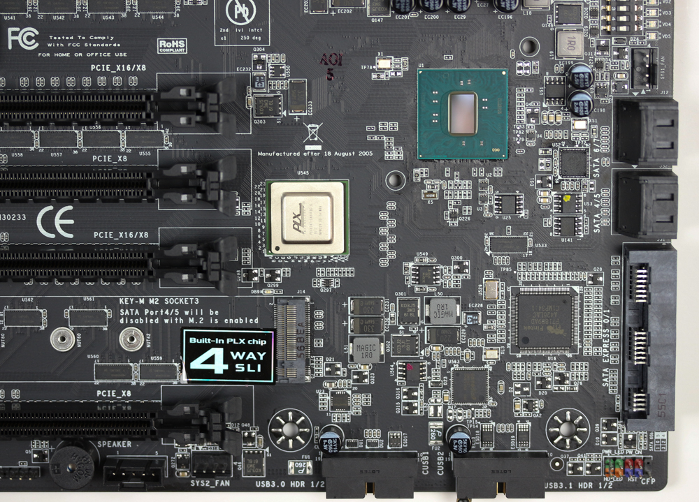
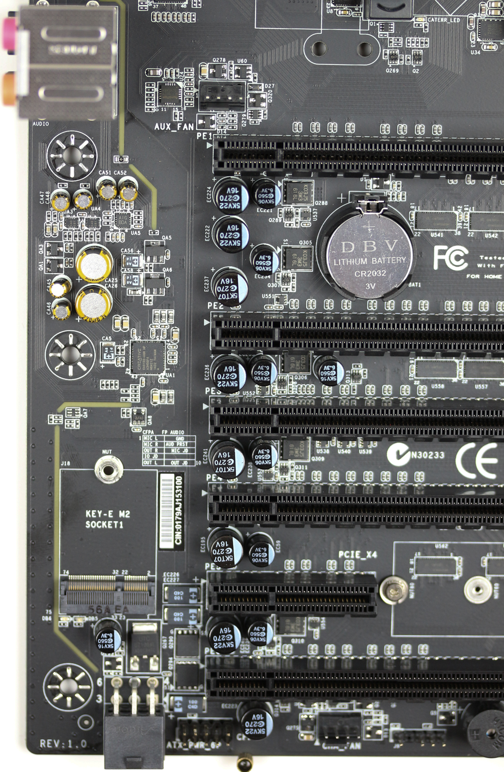
The board of course is EVGA’s top of the line board for the Z170 chipset and offers users a platform four-way SLI via a PLX chip. This definitely makes it stand out from the crowd for users who will want to run Skylake and a quad card setup. The look and layout of the board is really great with onboard power and reset buttons that seemed like it was mainly laid out for users who will install it in a case. Though they do throw us users who will be using it on the bench a bone with a dongle that has multiple voltage read points, that is the plug-in section right under the onboard buttons.
A closer look at the rest of the Z170 Classified motherboard
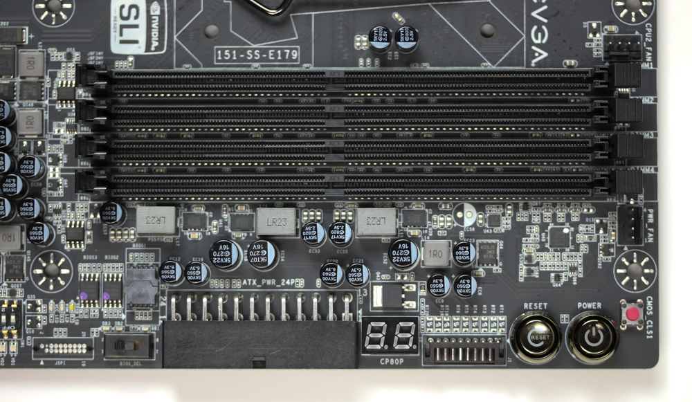
The post led, voltage read point dongle plug-in, onboard reset, oboard power, and clear cmos switch.
PLX chip and two M.2 slots, extra power for the PCI-E is provided by a 6-pin that is at a right angle as the main 24-pin power above.
A massive heatsink covers this part up and it sure should do a good job of keeping everything cool.
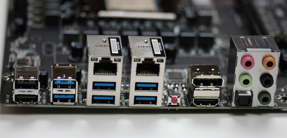
Looking at this from an overclocker’s point of view as well as a gamer I love that I see a clear cmos on the back but I really wish that they would have included at least a PS2 combo port.
Close up view
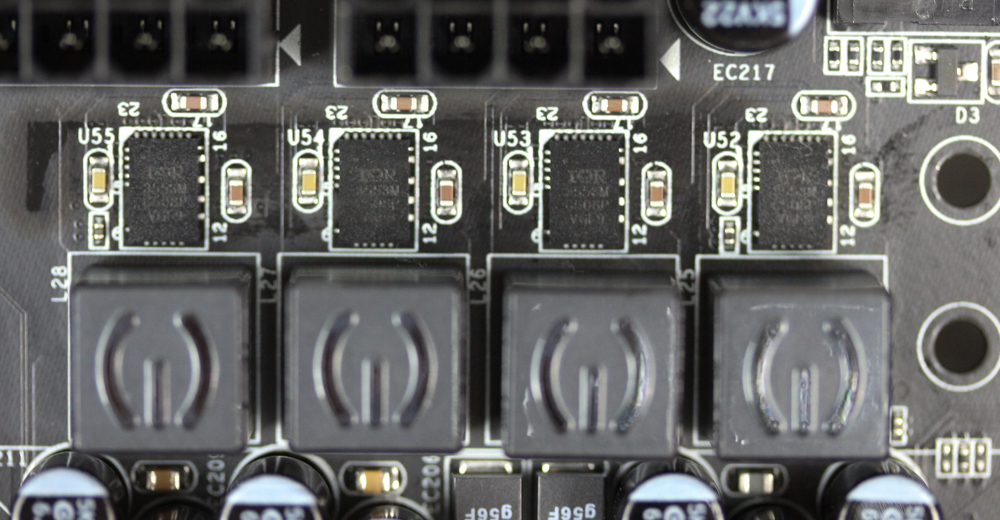
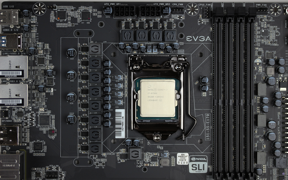
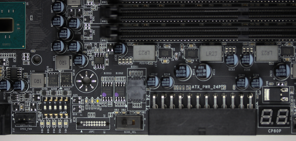
The VRM on this board is definitely over engineered which is always a great thing when you are looking to push something under ln2.
Audio section of the board
You can also see the two soldered BIOS chips and a third in a clamshell enclosure. These I have only seen on engineering sample boards that I have had the chance to work with and loved them. I think the thought here is if a user screws all three EVGA can easily send out a BIOS chip that they can easily drop in and get the board going, no puller tool needed.
Close up of the read points for voltages – best way to do it is to use the dongle that is included